- Jul 17, 2026
Share this post on:
The electronics industry is evolving faster than ever before, creating exciting career opportunities for students who want to build expertise in hardware design and embedded technologies. From consumer electronics and automotive systems to medical devices, aerospace, telecommunications, and IoT products, Printed Circuit Boards (PCBs) serve as the foundation of every electronic device.
According to industry reports, the global PCB market is projected to surpass US$ 110 billion by 2032, driven by rapid advancements in electric vehicles, IoT, industrial automation, AI-powered devices, and smart consumer electronics. This growing demand has made practical PCB design skills one of the most valuable assets for engineering students.
However, classroom learning alone is rarely enough to prepare students for real-world engineering challenges. Employers seek candidates who understand PCB layout principles, schematic design, signal integrity, manufacturing standards, testing procedures, and industry workflows. This is why choosing the right PCB design industrial training in Mohali can make a significant difference in your professional journey.
This comprehensive guide explains how to select the best industrial training in Mohali for students, what skills you should expect to learn, and why practical industry exposure plays an essential role in building a successful career in electronics.
Key Takeaways
- PCB design skills are highly demanded across multiple technology industries.
- Practical industrial exposure builds confidence beyond classroom learning.
- Live projects help students understand complete product development cycles.
- Professional software knowledge improves technical competency and employability.
- Experienced mentors accelerate learning through industry best practices.
- Choosing the right training partner significantly impacts long-term career growth.
Why PCB Design Industrial Training Matters for Your Career
PCB design is much more than arranging electronic components on a board. It involves careful planning, precision engineering, electrical analysis, thermal management, manufacturing considerations, and quality assurance. Industrial training helps students understand every stage of this engineering process.
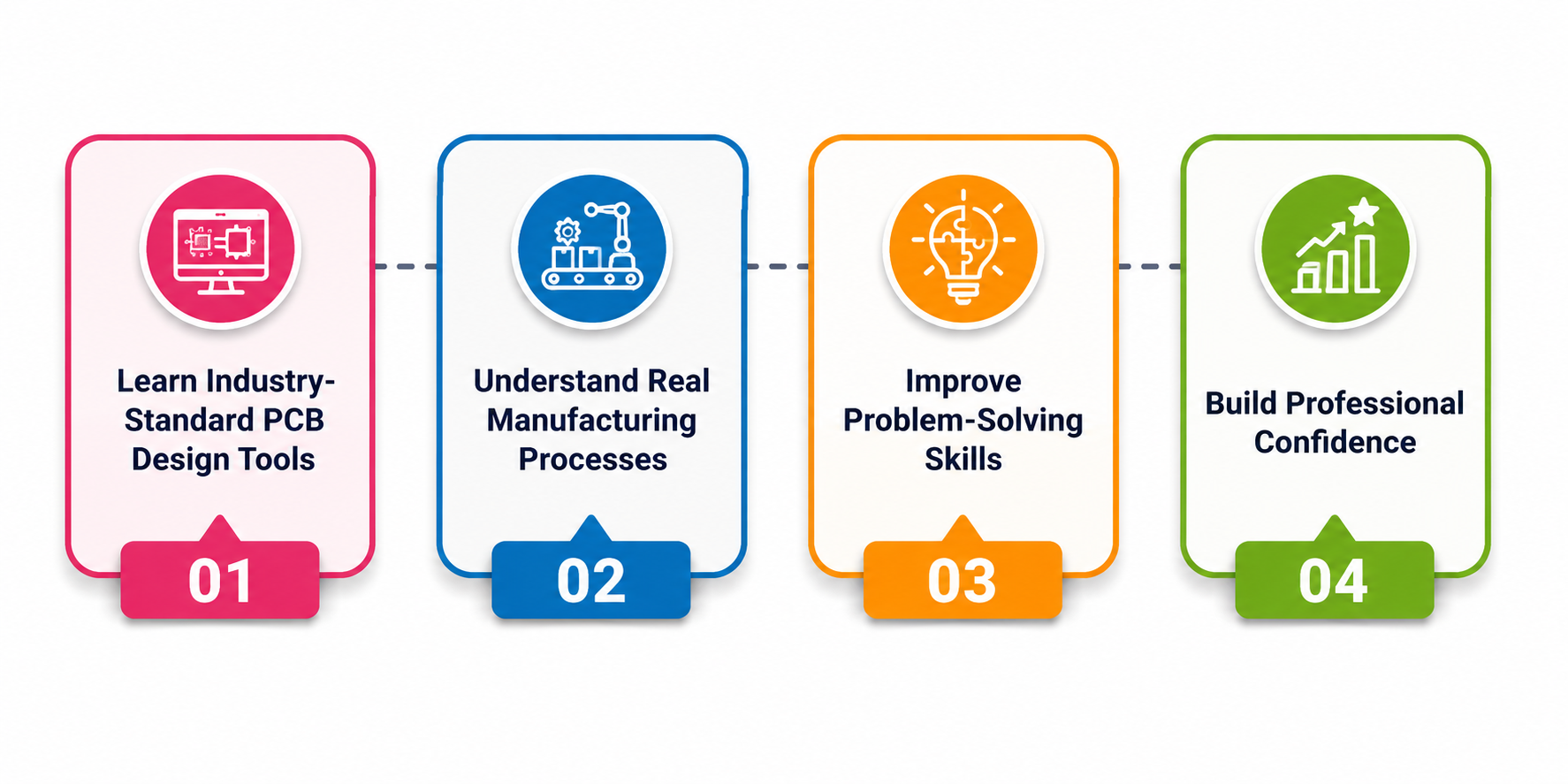
1. Learn Industry-Standard PCB Design Tools
Students gain practical exposure to professional PCB design software used by electronics companies worldwide. Learning these tools enables students to create production-ready PCB layouts while following modern engineering standards.
Benefits include:
- Designing multilayer circuit boards
- Creating accurate schematics
- Generating manufacturing files
- Understanding component libraries
2. Understand Real Manufacturing Processes
PCB design does not end after layout completion. Students also learn how their designs move toward manufacturing, assembly, inspection, and testing.
Practical exposure includes:
- PCB fabrication workflow
- Design rule verification
- Manufacturing constraints
- Assembly considerations
3. Improve Problem-Solving Skills
Industrial environments present real engineering challenges that cannot be replicated in textbooks. Students learn how to identify design flaws, troubleshoot issues, optimize layouts, and improve overall circuit performance.
Important learning areas include:
- Signal routing optimization
- Power distribution analysis
- Noise reduction techniques
- Hardware debugging
4. Build Professional Confidence
Working on industry-oriented projects gives students the confidence to contribute to engineering teams after graduation. Employers value candidates who already understand professional workflows.
The confidence grows through:
- Live project participation
- Team collaboration
- Technical presentations
- Independent design assignments
How to Choose the Best PCB Design Industrial Training
Selecting the right training program requires careful evaluation. Students should focus on practical learning opportunities rather than simply completing theoretical sessions. A quality Best industrial training in Chandigarh experience should prepare students for industry expectations while enhancing both technical and professional skills.
1. Experienced Industry Mentors
Learning from professionals who have worked on commercial PCB projects provides valuable insights into current industry practices. Look for mentors who can teach:
- Modern PCB design techniques
- Hardware troubleshooting
- Product development lifecycle
- Industry documentation standards
2. Live Project Experience
Hands-on learning remains one of the most important factors when selecting training. Students should work on real PCB projects instead of only following demonstrations. Live projects may include:
- Embedded hardware systems
- IoT circuit boards
- Consumer electronics
- Industrial automation hardware
3. Practical Learning Environment
An effective training environment encourages experimentation, innovation, and problem-solving. Students should receive opportunities for:
- Individual projects
- Team assignments
- Hardware testing
- Prototype development
4. Updated Curriculum
Electronics technology evolves rapidly. Training should include current industry practices rather than outdated concepts. Modern topics may include:
- High-speed PCB design
- IoT hardware integration
- Embedded systems
- PCB simulation
- EMI and EMC fundamentals
5. Industry-Oriented Project Portfolio
By the end of training, students should have a portfolio demonstrating their engineering capabilities. A strong portfolio includes:
- PCB layouts
- Circuit schematics
- Manufacturing files
- Technical documentation
6. Placement Assistance
Many students choose Industrial training in Chandigarh because it also supports career development through interview preparation and placement guidance. Useful career support includes:
- Resume building
- Technical interview preparation
- Mock interviews
- Career counseling
Essential Skills You Should Learn During PCB Design Industrial Training
The objective of PCB design industrial training extends beyond software proficiency. Students should understand the complete engineering lifecycle involved in PCB development. A comprehensive program prepares students for various hardware engineering roles across industries.
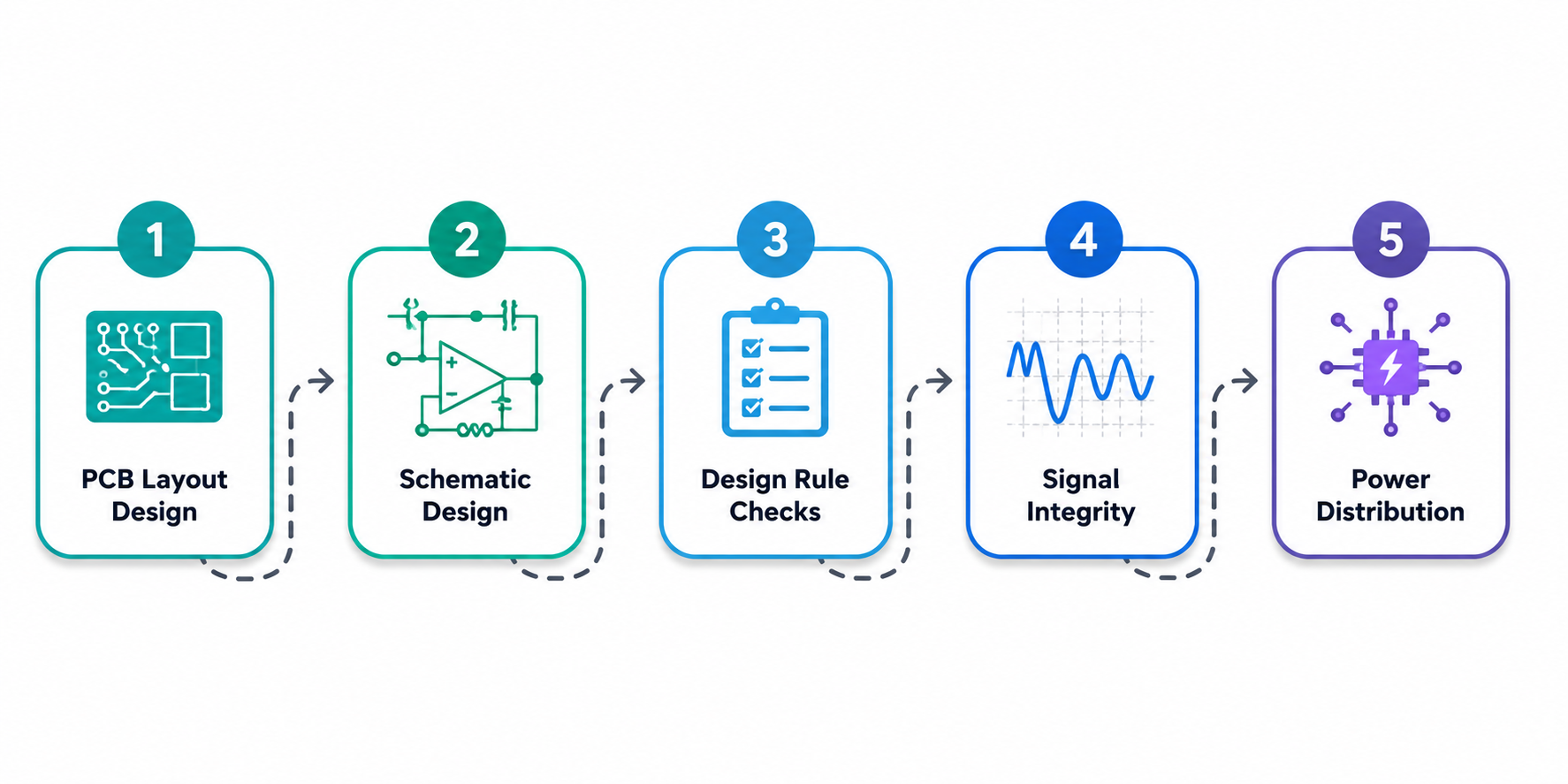
1. PCB Layout Design
PCB layout design is one of the most critical skills students develop during industrial training. It involves strategically placing electronic components and routing electrical connections while ensuring optimal performance, manufacturability, and reliability. Students learn industry best practices for designing single-layer, double-layer, and multilayer PCBs while considering factors such as spacing, trace width, thermal management, and component placement.
2. Schematic Design
Before creating a PCB layout, engineers must develop an accurate electronic schematic that represents the circuit's functionality. During industrial training, students learn how to create professional schematics, select appropriate electronic components, define electrical connections, and organize circuit architecture efficiently.
3. Design Rule Checks
Design Rule Checks (DRC) play a crucial role in ensuring that PCB designs comply with manufacturing standards and engineering specifications. Students learn how to identify and resolve issues such as insufficient clearances, incorrect trace widths, overlapping components, and routing violations before sending designs for fabrication.
4. Signal Integrity
As electronic devices become faster and more complex, maintaining signal integrity has become an essential aspect of PCB design. Industrial training introduces students to techniques that minimize signal distortion, electromagnetic interference (EMI), crosstalk, and transmission delays. Students learn routing strategies, impedance considerations, differential pair design, and grounding techniques that help maintain reliable signal performance and communication circuits.
5. Power Distribution
Efficient power distribution is fundamental to achieving stable and reliable PCB performance. During training, students learn how to design effective power delivery networks that ensure consistent voltage levels across electronic components while minimizing electrical noise and voltage drops.
Benefits of PCB Design Industrial Training
PCB design industrial training in Mohali provides much more than technical knowledge - it equips students with the practical experience, industry exposure, and professional skills needed to succeed in today's competitive electronics sector.
1. Better Career Opportunities
One of the biggest advantages of PCB design industrial training is the access it provides to a wide range of career opportunities. Employers increasingly seek candidates who possess practical knowledge of PCB design, electronic circuit development, and hardware engineering workflows rather than relying solely on academic qualifications. Through industrial training, students become familiar with industry-standard tools, development practices, and project execution, making them more attractive to recruiters.
2. Practical Engineering Knowledge
Industrial training bridges the gap between classroom learning and real-world engineering applications. Instead of focusing only on theoretical concepts, students gain hands-on experience in designing, developing, testing, and validating PCB layouts for practical electronic systems. They learn how engineering decisions impact product performance, manufacturing efficiency, and overall system reliability.
3. Improved Resume
A strong technical resume plays a significant role in securing internships and job opportunities, and industrial training helps students build an impressive professional portfolio. Employers highly value candidates who can demonstrate practical experience through completed projects rather than only listing academic qualifications. Hands-on training allows students to showcase their technical abilities and problem-solving capabilities with confidence.
4. Enhanced Problem-Solving Skills
Every engineering project presents unique challenges, and industrial training teaches students how to solve them systematically. Working on real-world PCB design projects exposes students to practical issues such as routing conflicts, component placement limitations, thermal management, signal interference, manufacturing constraints, and hardware debugging. Learning to identify and resolve these challenges strengthens both technical expertise and critical thinking abilities.
Career Opportunities After PCB Design Industrial Training
The demand for skilled PCB design professionals continues to grow as industries invest in advanced electronics, automation, IoT, and smart devices. Completing PCB design industrial training equips students with practical skills that open doors to diverse career opportunities across multiple sectors.
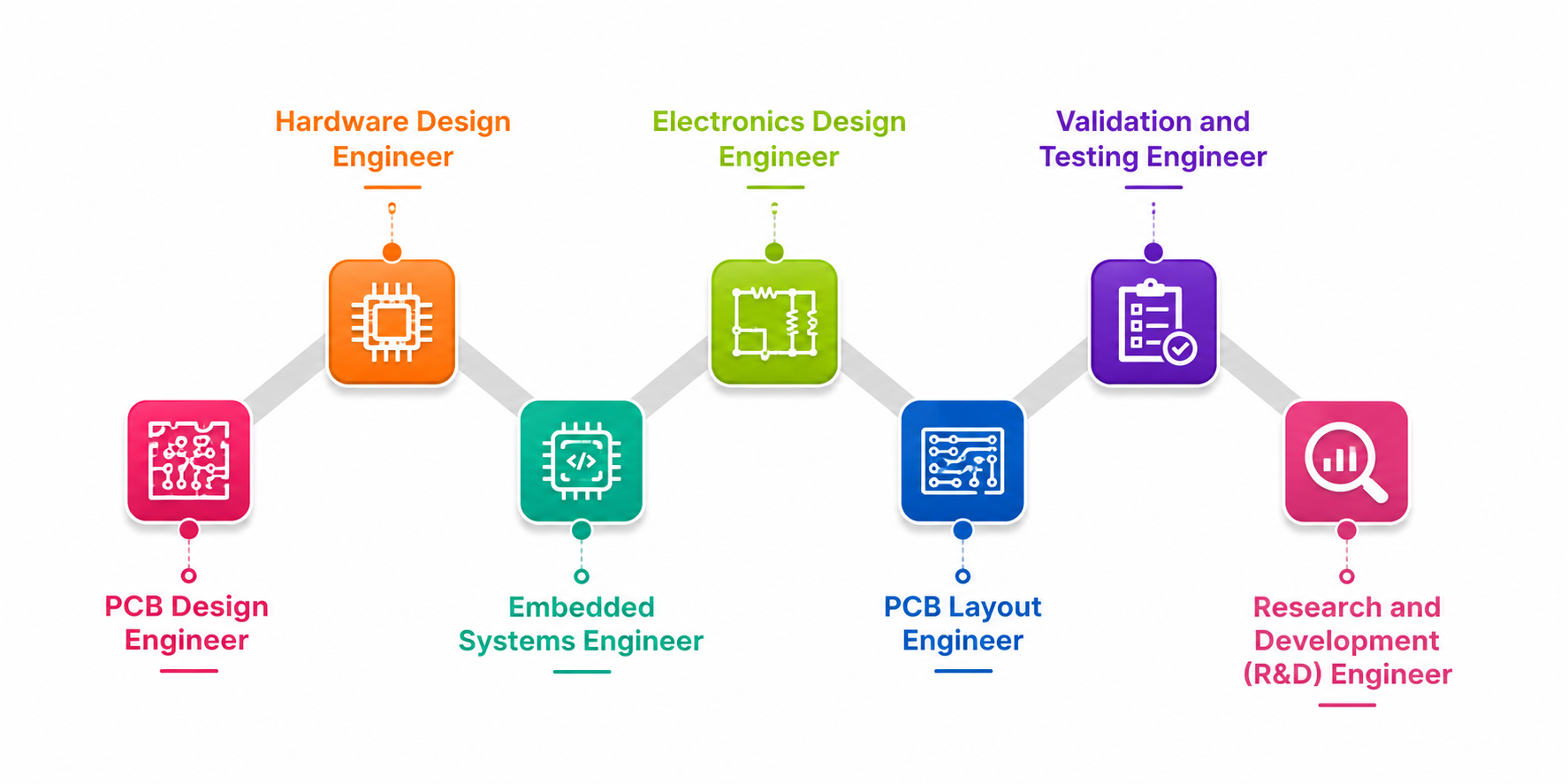
1. PCB Design Engineer
PCB Design Engineers create circuit board layouts, optimize component placement, and ensure designs meet manufacturing and performance standards. They work closely with hardware and embedded teams to develop reliable electronic products.
2. Hardware Design Engineer
Hardware Design Engineers develop electronic circuits and hardware systems for consumer electronics, industrial equipment, automotive applications, and medical devices. PCB design knowledge serves as a strong foundation for this role.
3. Embedded Systems Engineer
Embedded Systems Engineers integrate hardware with software to develop intelligent electronic products. A solid understanding of PCB design helps professionals create efficient and reliable embedded solutions.
4. Electronics Design Engineer
Electronics Design Engineers are responsible for designing, testing, and improving electronic systems. They work on circuit development, prototype testing, and product optimization across various industries.
5. PCB Layout Engineer
PCB Layout Engineers specialize in designing high-quality board layouts while ensuring signal integrity, thermal performance, and manufacturability. They collaborate with electrical engineers to produce production-ready designs.
6. Validation and Testing Engineer
Validation Engineers test and verify PCB assemblies to ensure they meet design specifications and quality standards. They identify issues, troubleshoot hardware problems, and support product reliability.
7. Research and Development (R&D) Engineer
R&D Engineers work on innovative electronic products by exploring new technologies, improving existing designs, and developing advanced hardware solutions. PCB design expertise is valuable for creating next-generation products.
Why Students Choose ToXSL Technologies for Industrial Training?
Thousands of engineering students aim to acquire practical industry knowledge before beginning their professional careers. ToXSL Technologies has established itself as a trusted technology company by offering hands-on industrial training focused on real business requirements rather than only theoretical concepts. Students looking for Industrial training in Mohali benefit from an industry-driven learning environment where practical implementation, mentorship, and project-based learning are prioritized. Here are some of the reasons students choose ToXSL Technologies:
1. Industry-Focused Practical Learning
Students work on real-time projects that simulate professional development environments, allowing them to understand the complete PCB design lifecycle from schematic creation to manufacturing-ready layouts.
2. Experienced Technical Mentors
Training is conducted by experienced professionals who guide students through practical engineering challenges, helping them understand industry standards, troubleshooting techniques, and best development practices.
3. Live Project Exposure
Students gain valuable experience by participating in live projects that strengthen technical knowledge while improving confidence and analytical thinking.
4 Modern Development Environment
The training environment incorporates current tools, technologies, and engineering methodologies to ensure students remain aligned with modern industry expectations.
5. Professional Skill Development
Along with technical learning, students improve communication, teamwork, documentation, presentation, and project management skills that employers highly value.
6. Career Preparation
ToXSL Technologies also supports students with resume preparation, interview guidance, technical discussions, and professional career advice to improve placement opportunities.
Conclusion
PCB design continues to play a vital role in the rapidly expanding electronics industry. As businesses increasingly invest in smart devices, automation systems, IoT solutions, medical equipment, and electric vehicles, the demand for skilled PCB design professionals will continue to grow. Students who combine strong academic knowledge with practical industrial experience gain a competitive advantage in today's job market.
At ToXSL Technologies, we believe that effective industrial training goes beyond learning software tools. Our objective is to help students develop practical engineering skills through live projects, expert mentorship, real-world problem-solving, and professional guidance. Whether you are looking for the best industrial training for students or planning your career in electronics, our industry-focused training approach is designed to prepare you for long-term professional success and help you confidently step into the world of hardware innovation.
Frequently Asked Questions
1. Who should join PCB Design Industrial Training?
PCB design industrial training is ideal for students pursuing Electronics Engineering, Electrical Engineering, Embedded Systems, Mechatronics, Instrumentation, and related technical disciplines who want practical industry exposure.
2. Why is industrial training important for PCB design?
Industrial training helps students apply theoretical concepts to real-world projects, understand professional engineering workflows, gain practical experience, and improve employability.
3. What skills can students develop during PCB design industrial training?
Students typically learn schematic design, PCB layout, component placement, routing techniques, design rule checks, manufacturing documentation, hardware testing, troubleshooting, and project documentation.
4. How does practical project experience benefit engineering students?
Working on live projects improves technical confidence, problem-solving abilities, teamwork, communication skills, and helps students build an impressive professional portfolio for future job opportunities.
5. How can ToXSL Technologies help students build a successful electronics career?
ToXSL Technologies provides hands-on industrial training, experienced mentorship, live project exposure, modern development practices, interview preparation, and career guidance to help students become industry-ready professionals.